Several times I was rescued by power supplies, the circuits of which have already become classic, remaining simple for anyone who has soldered something electronic at least once in their life.
Similar circuits were developed by many radio amateurs for different purposes, but each designer put something of his own into the circuit, changed calculations, individual components of the circuit, conversion frequency, power, adjusting to some needs known only to the author himself ...
I often had to use such circuits instead of their bulky transformer counterparts, lightening the weight and volume of my designs, which needed to be powered from the mains. As an example: a stereo amplifier on a microcircuit, assembled in a duralumin case from an old modem.
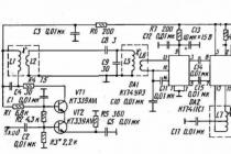
The description of the operation of the circuit, since it is classical, does not make much sense. I will only note that I refused to use a transistor operating in the avalanche breakdown mode as a trigger circuit, because. unijunction transistors type KT117 work in the launch node much more reliably. I also like running on a dinistor.


The figure shows: a) the pinout of old KT117 transistors (without tongue), b) the modern pinout of KT117, c) the layout of the pins on the circuit, d) an analogue of a unijunction transistor on two ordinary ones (any transistors of the correct structure - p-n-p (VT1) structures such as KT208, KT209, KT213 will do , KT361, KT501, KT502, KT3107; n-p-n (VT2) structures such as KT315, KT340, KT342, KT503, KT3102)
UPS circuit on bipolar transistors

FET UPS circuit
The circuit on field-effect transistors is somewhat more complicated, which is caused by the need to protect their gates from overvoltage.
Error. Diode VD1 turn on the other way around!
All winding data of transformers are shown in the figures. The maximum load power that can be powered by a power supply with a transformer made on a 3000NM 32 × 16X8 ferrite ring is about 70W, on a K40 × 25X11 of the same brand - 150W.
Diode VD1 in both circuits, disables the trigger circuit by applying a negative voltage to the unijunction transistor emitter after the converter has started.
Of the features- power supply units are switched off by closing the winding II of the switching transformer. In this case, the lower transistor according to the circuit is locked and generation is disrupted. But, by the way, the disruption of generation occurs precisely because of the “short-circuiting” of the winding.
The locking of the transistor in this case, although it obviously occurs due to the closure of the emitter junction by the contact of the switch, is secondary. The unijunction transistor in this case will not be able to start the converter, which can be in this state (both keys are locked in direct current through practically zero resistance of the transformer windings) for an arbitrarily long time.
A properly calculated and carefully assembled power supply design, as a rule, easily starts under the required load and behaves stably in operation.
Constantine (riswel)
Russia, Kaliningrad
Since childhood - music and electro / radio equipment. Soldered a lot of schemes of the most diverse for various reasons, and simply - for the sake of interest - both my own and others'.
For 18 years of work in North-West Telecom, he has manufactured many different stands for testing various equipment being repaired.
He designed several, different in functionality and element base, digital pulse duration meters.
More than 30 rationalization proposals for the modernization of units of various specialized equipment, incl. - power supply. For a long time I have been more and more engaged in power automation and electronics.
Why am I here? Yes, because everyone here is the same as me. There are a lot of interesting things for me here, since I am not strong in audio technology, but I would like to have more experience in this particular direction.
Or create a winding, you can assemble a pulse-type power supply with your own hands, which requires a transformer with just a few turns.
At the same time, a small number of parts will be required, and the work can be completed in 1 hour. In this case, the IR2151 chip is used as the basis for the power supply.
To work, you will need the following materials and parts:
- PTC thermistor any type.
- A pair of capacitors, which are selected with the calculation of 1 microfarad. at 1 W. When creating a design, we select capacitors so that they draw 220 watts.
- diode assembly vertical type.
- Drivers type IR2152, IR2153, IR2153D.
- FETs type IRF740, IRF840. You can choose others if they have a good resistance indicator.
- Transformer can be taken from old computer system units.
- Diodes installed at the output, it is recommended to take from the HER family.
In addition, you will need the following tools:
- soldering iron and consumables.
- Screwdriver and pliers.
- Tweezers.
Also, do not forget about the need for good lighting in the workplace.
Step-by-step instruction
 circuit diagram
  structural scheme
 The assembly is carried out according to the drawn up circuit diagram. The microcircuit was selected according to the features of the circuit.
Assembly is carried out as follows:
- At the entrance install PTC thermistor and diode bridges.
- Then, a pair of capacitors is installed.
- Drivers necessary to regulate the operation of the gates of field-effect transistors. If the drivers have index D at the end of the marking, it is not necessary to install FR107.
- FETs installed without shorting the flanges. When mounting to a radiator, special insulating gaskets and washers are used.
- transformers installed with shorted leads.
- diode output.
All elements are installed in the designated places on the board and soldered on the reverse side.
Examination
 In order to correctly assemble the power supply, you need to carefully consider the installation of polar elements, and you should also be careful when working with mains voltage. After disconnecting the unit from the power source, no dangerous voltage should remain in the circuit. With proper assembly, subsequent adjustment is not carried out.
You can check the correct operation of the power supply as follows:
- Include in the chain the output is a light bulb, for example, 12 volts. At the first short start, the light should be on. In addition, you should pay attention to the fact that all elements should not heat up. If something is heating up, then the circuit is assembled incorrectly.
- At the second start measure the current value with a tester. We give the block enough time to work in order to make sure that there are no heating elements.
In addition, it would be useful to check all the elements with a tester for the presence of high current after turning off the power.
- As previously noted, the operation of the switching power supply is based on feedback. The scheme under consideration does not require a special organization of feedback and various power filters.
- Particular attention should be paid to the choice of field-effect transistors. In this case, IR FETs are recommended, which are renowned for their resistance to thermal resolution. According to the manufacturer, they can work stably up to 150 degrees Celsius. However, in this scheme they do not heat up much, which can be called a very important feature.
- If the heating of transistors occurs constantly, active cooling should be installed. As a rule, it is represented by a fan.
Advantages and disadvantages

The pulse converter has the following advantages:
- High rate stabilization coefficient allows you to provide power conditions that will not harm sensitive electronics.
- Designs under consideration have a high efficiency. Modern versions have this indicator at the level of 98%. This is due to the fact that losses are reduced to a minimum, as evidenced by the low heating of the unit.
- Large input voltage range- one of the qualities due to which such a design has spread. At the same time, the efficiency does not depend on the input current indicators. It is the immunity to the voltage indicator that makes it possible to extend the life of the electronics, since jumps in the voltage indicator are a frequent occurrence in the domestic power supply network.
- Incoming current frequency affects the operation of only the input elements of the structure.
- Small dimensions and weight, also cause popularity due to the proliferation of portable and portable equipment. Indeed, when using a linear block, the weight and dimensions increase several times.
- Organization of remote control.
- Less cost.
There are also disadvantages:
- Availability impulse interference.
- Necessity inclusion in the circuit of power factor compensators.
- Complexity self regulation.
- Less reliable due to the complexity of the circuit.
- Severe consequences when one or more circuit elements exit.
When creating such a design on your own, it should be borne in mind that the mistakes made can lead to failure of the electrical consumer. Therefore, it is necessary to provide for the presence of protection in the system.
Device and features of work

When considering the features of the operation of the pulse unit, the following can be noted:
- At first the input voltage is rectified.
- Rectified voltage depending on the purpose and features of the whole structure, it is redirected in the form of a high-frequency rectangular pulse and fed to an installed transformer or filter operating at low frequencies.
- transformers are small in size and weight when using a pulse block due to the fact that increasing the frequency allows you to increase the efficiency of their work, as well as reduce the thickness of the core. In addition, a ferromagnetic material can be used in the manufacture of the core. At low frequency, only electrical steel can be used.
- Voltage stabilization occurs through negative feedback. Through the use of this method, the voltage supplied to the consumer remains unchanged, despite fluctuations in the input voltage and the load created.
Feedback can be organized as follows:
- With galvanic isolation, optocoupler or transformer winding output is used.
- If you do not need to create a decoupling, a resistor voltage divider is used.
In similar ways, the output voltage is maintained with the desired parameters.
Standard switching power supplies, which can be used, for example, to regulate the output voltage when powered , consists of the following elements:
- Input part, high voltage. It is usually represented by a pulse generator. The pulse width is the main indicator that affects the output current: the wider the indicator, the greater the voltage, and vice versa. The pulse transformer stands on the section of the input and output parts, conducts the selection of the pulse.
- There is a PTC thermistor on the output side.. It is made of a semiconductor and has a positive temperature coefficient. This feature means that when the temperature of the element rises above a certain value, the resistance indicator rises significantly. Used as a security key mechanism.
- Low voltage part. A pulse is removed from the low-voltage winding, rectification occurs using a diode, and the capacitor acts as a filter element. The diode assembly can rectify the current up to 10A. It should be borne in mind that capacitors can be designed for different loads. The capacitor carries out the removal of the remaining pulse peaks.
- Drivers carry out the damping of the resulting resistance in the power circuit. During operation, the drivers alternately open the gates of the installed transistors. Work occurs at a certain frequency
- FETs are chosen taking into account the resistance indicators and the maximum voltage in the open state. At a minimum value, the resistance significantly increases efficiency and reduces heating during operation.
- Standard transformer for downgrade.
Given the selected scheme, you can begin to create a power supply of the type in question.
Good afternoon My opinion: The scheme (first) will work, everything you need is there! Tips to replace the driver, add capacity, etc. there are unfounded. If something is changed, then this is a separate scheme and other discussions. The weak point is capacitors with a midpoint of 200 V! Yes, it will work, but if the capacitor could, he expressed his desire to increase the breakdown voltage to 350 V! It's just a filter - half the trouble, but decoupling the load and working on the transformer winding is another. We consider, and who is not too lazy: 310 V (for example, power supply) + 150 V (EMF of the transformer inductance discharge) = 460 V. Half equals 230 volts. Or maybe "BOOM!" - maybe, but it will be "p-sh-sh-sh-i-k!" and the capacitor will leak. Like clearly explained. And the scheme will work and give what it was counted on! Fact! Protection! The best defense is the one that is simple! Those. fuse both at the inlet and outlet. The fuse operation speed is sufficient for the key pulse current time of 25 A! Do you understand that this is enough? Enough. To obtain maximum efficiency, you need to select the pulse frequency for the transformer used, this is obvious. ferrite was heated to 100 gr. lost properties, the calculation will be adjusted. How to choose is easy. We measure the current consumption of the circuit after the rectifier. By changing the frequency from higher to lower, we find the moment of current increase - stop! We increase the frequency by 1-2 kHz. All! How to change the frequency? Simply, replace the resistor Rt with a trimmer of greater resistance (without fanaticism). You also need to select the frequency for the transformer from the computer's power supply. The spread of operating frequencies from 32 kHz to 55 kHz. Success to all. As for the second scheme, this is a variant of all the errors of the first and some other schemes from the Internet! Why? The first and most important in the "datasheet" IR2153 IRF740 are clear contradictions: the breakdown voltage is not less than 600 V. and the keys are 400v. The gate capacitance for 2153 (load) is no more than 1000 pF, and for 740 = 1400 pF. Yes, the bulbs will glow, but with this block you are doomed to purchase more than one set of parts. The output voltage will sag - there is no required pulse steepness. The efficiency will be below the maximum, we warm the environment. In general, the selection of parts of the (second) circuit is a mistake! The 740 requires a 2155 driver (manufacturer's recommendation) capacitance up to 2200 pf in load. The scheme is an experiment with an explosion! Collect strictly with glasses and gloves! What would I put together? Keys STP5NK60C (or 4NK60, 6NK60, 7NK60...)< 1000 пф. Остальное все рабочее, правда я бы подобрал частоту и ток драйвера как описал выше. Напомню: запас в электронике не всегда уместен. Скажем взять ключи на пробой в 1000 в - это неправильно. IRF740 - отличные ключи для применения в Китае, напряжение сети 110 - 120 в. Как то так.
The scope of switching power supplies in everyday life is constantly expanding. Such sources are used to power all modern household and computer equipment, to implement uninterruptible power supplies, chargers for batteries for various purposes, to implement low-voltage lighting systems, and for other needs.
In some cases, buying a ready-made power supply is not very acceptable from an economic or technical point of view, and assembling a switching power supply with your own hands is the best way out of this situation. Simplifies this option and the wide availability of modern element base at low prices.
The most popular in everyday life are switching sources powered by a standard AC network and a powerful low-voltage output. The block diagram of such a source is shown in the figure.
The mains rectifier CB converts the alternating voltage of the supply network into a constant one and smoothes out the ripples of the rectified voltage at the output. The high-frequency VChP converter converts the rectified voltage into an alternating or unipolar one, having the form of rectangular pulses of the required amplitude.
In the future, such a voltage either directly or after rectification (HV) is supplied to a smoothing filter, to the output of which a load is connected. The VChP is controlled by a control system that receives a feedback signal from the load rectifier.
Such a structure of the device can be criticized due to the presence of several conversion links, which reduces the efficiency of the source. However, with the right choice of semiconductor elements and high-quality calculation and manufacture of coil units, the level of power losses in the circuit is small, which makes it possible to obtain real values of efficiency above 90%.
Schematic diagrams of switching power supplies
Structural block solutions include not only the rationale for choosing circuit implementation options, but also practical recommendations for choosing the main elements.
To rectify the mains single-phase voltage, one of the three classic schemes shown in the figure is used:
- half-wave;
- zero (two-half-wave with a midpoint);
- two-half-wave bridge.

Each of them has advantages and disadvantages that determine the scope.
Half wave circuit characterized by ease of implementation and a minimum number of semiconductor components. The main disadvantages of such a rectifier are a significant amount of output voltage ripple (in the rectified one there is only one half-wave of the mains voltage) and a low rectification factor.
Rectification ratio Kv determined by the ratio of the average value of the voltage at the output of the rectifier Udk effective value of the phase mains voltage Uph.
For a half-wave circuit, Kv \u003d 0.45.
To smooth out the ripple at the output of such a rectifier, powerful filters are required.
Zero, or full-wave circuit with a midpoint, although it requires a double number of rectifier diodes, however, this disadvantage is largely offset by a lower level of rectified voltage ripple and an increase in the rectification factor to 0.9.
The main disadvantage of such a scheme for use in domestic conditions is the need to organize the midpoint of the mains voltage, which implies the presence of a mains transformer. Its dimensions and weight turn out to be incompatible with the idea of a small-sized self-made pulsed source.
full wave bridge rectification has the same indicators in terms of ripple level and rectification factor as the zero circuit, but does not require a network. This compensates for the main drawback - twice the number of rectifier diodes, both in terms of efficiency and cost.
To smooth out the ripple of the rectified voltage, the best solution is to use a capacitive filter. Its use allows you to raise the value of the rectified voltage to the amplitude value of the mains (at Uph=220V Ufm=314V). The disadvantages of such a filter are considered to be large values of the pulsed currents of the rectifier elements, but this disadvantage is not critical.
The choice of rectifier diodes is carried out according to the average forward current Ia and the maximum reverse voltage U BM.
Taking the value of the output voltage ripple coefficient Kp=10%, we obtain the average value of the rectified voltage Ud=300V. Taking into account the load power and the efficiency of the RF converter (80% is taken for calculation, but in practice it will turn out higher, this will allow you to get some margin).
Ia is the average current of the rectifier diode, Рн is the load power, η is the efficiency of the RF converter.
The maximum reverse voltage of the rectifier element does not exceed the amplitude value of the mains voltage (314V), which allows the use of components with a value of U BM =400V with a significant margin. You can use both discrete diodes and ready-made rectifier bridges from various manufacturers.
To ensure a given (10%) ripple at the rectifier output, the capacitance of the filter capacitors is taken at the rate of 1 μF per 1 W of output power. Electrolytic capacitors with a maximum voltage of at least 350V are used. Filter capacities for various capacities are shown in the table.

High frequency converter: its functions and circuits
The high-frequency converter is a single-cycle or two-cycle key converter (inverter) with a pulse transformer. Variants of circuits of RF converters are shown in the figure.

Single cycle circuit. With a minimum number of power elements and ease of implementation, it has several disadvantages.
- The transformer in the circuit operates on a private hysteresis loop, which requires an increase in its size and overall power;
- To provide output power, it is necessary to obtain a significant amplitude of the pulsed current flowing through the semiconductor switch.
The scheme has found the greatest application in low-power devices, where the influence of these disadvantages is not so significant.
 To change or install a new meter yourself, no special skills are required. Choosing the right one will ensure that the current consumed is correctly accounted for and will increase the safety of the home electrical network.
In modern lighting conditions, both indoors and outdoors, motion sensors are increasingly being used. This gives not only comfort and convenience to our homes, but also allows you to save a lot. You can find out practical tips on choosing an installation site, connection diagrams.
Push-Pull Circuit with Transformer Midpoint (Push-Pull). It got its second name from the English version (push-pull) of the job description. The circuit is free from the shortcomings of the single-cycle version, but has its own - a complicated design of the transformer (it is required to manufacture identical sections of the primary winding) and increased requirements for the maximum voltage of the switches. Otherwise, the solution deserves attention and is widely used in do-it-yourself switching power supplies and not only.
Push-Pull Half-Bridge. In terms of parameters, the circuit is similar to the circuit with a midpoint, but does not require a complex configuration of the transformer windings. The inherent disadvantage of the circuit is the need to organize the middle point of the rectifier filter, which entails a fourfold increase in the number of capacitors.
Due to the ease of implementation, the circuit is most widely used in switching power supplies up to 3 kW. At high powers, the cost of the filter capacitors becomes unacceptably high compared to the semiconductor switches of the inverter, and the bridge circuit turns out to be the most profitable.
Push-Pull Bridge. Similar in parameters to other push-pull circuits, but without the need to create artificial "midpoints". The price for this is a doubled number of power switches, which is beneficial from an economic and technical point of view for building powerful pulsed sources.
The choice of inverter keys is carried out according to the amplitude of the collector (drain) current I KMAX and the maximum collector-emitter voltage U KEMAC. For the calculation, the load power and the transformation ratio of the pulse transformer are used.
However, first you need to calculate the transformer itself. The pulse transformer is made on a core made of ferrite, permalloy or transformer iron twisted into a ring. For powers up to units of kW, ferrite cores of an annular or W-shaped type are quite suitable. The calculation of the transformer is based on the required power and conversion frequency. To exclude the appearance of acoustic noise, it is desirable to move the conversion frequency outside the audio range (make it higher than 20 kHz).
At the same time, it must be remembered that at frequencies close to 100 kHz, losses in ferrite magnetic circuits increase significantly. The calculation of the transformer itself is not difficult and can be easily found in the literature. Some results for various power sources and magnetic cores are shown in the table below.
The calculation was made for a conversion frequency of 50 kHz. It is worth noting that when operating at a high frequency, the effect of current displacement to the surface of the conductor takes place, which leads to a decrease in the effective winding area. To prevent this kind of trouble and reduce losses in conductors, it is necessary to wind from several cores of a smaller cross section. At a frequency of 50 kHz, the permissible diameter of the winding wire does not exceed 0.85 mm.
![]()
Knowing the load power and the transformation ratio, it is possible to calculate the current in the primary winding of the transformer and the maximum collector current of the power switch. The voltage on the transistor in the closed state is selected higher than the rectified voltage supplied to the input of the RF converter with a certain margin (U KEMAH>=400V). Based on this data, keys are selected. Currently, the best option is to use IGBT or MOSFET power transistors.
For rectifier diodes on the secondary side, one rule must be observed - their maximum operating frequency must exceed the conversion frequency. Otherwise, the efficiency of the output rectifier and the converter as a whole will be significantly reduced.
Video on the manufacture of the simplest switching power supply
6) I plan to implement a power transformer on an Epcos ETD44/22/15 type core made of N95 material. Perhaps my choice will change further when I calculate winding data and overall power.
7) I hesitated for a long time between choosing the type of rectifier on the secondary winding between a dual Schottky diode and a synchronous rectifier. You can put a dual Schottky diode, but this is P \u003d 0.6V * 40A \u003d 24 W in heat, with a SMPS power of about 650 W, a loss of 4% is obtained! When using the most common IRF3205 in a synchronous rectifier with a resistance channel, heat will be released P = 0.008 ohm * 40A * 40A = 12.8W. It turns out we win 2 times or 2% efficiency! Everything was beautiful until I put together a solution on the breadboard on the IR11688S. Dynamic switching losses were added to the static losses on the channel, and in the end, that's what happened. The capacitance of field workers for high currents is still large. this is treated with drivers like HCPL3120, but this is an increase in the price of the product and an excessive complication of circuitry. Actually, from these considerations, it was decided to put a double Schottky and sleep peacefully.
8) The LC circuit at the output, firstly, will reduce the current ripple, and secondly, it will allow you to “cut off” all harmonics. The latter problem is extremely relevant when powering devices operating in the radio frequency range and incorporating high-frequency analog circuits. In our case, we are talking about a HF transceiver, so here the filter is simply vital, otherwise the interference will “crawl” into the air. Ideally, you can still put a linear stabilizer on the output and get minimal ripples in units of mV, but in fact, the speed of the OS will allow you to get voltage ripples within 20-30 mV without a “boiler”, inside the transceiver, critical nodes are powered through their LDOs, so its redundancy is obvious.
Well, we ran through the functionality and this is just the beginning)) But nothing, it will go more cheerfully, because the most interesting part begins - the calculations of everything and everything!
Calculation of a power transformer for a half-bridge voltage converter
Now it's worth thinking a little about the construct and topology. I plan to use field effect transistors, not IGBTs, so you can choose a larger operating frequency, while I'm thinking about 100 or 125 kHz, the same frequency will be on KKM by the way. Increasing the frequency will slightly reduce the dimensions of the transformer. On the other hand, I don’t want to turn up the frequency much, because I use TL494 as a controller, after 150 kHz it does not show itself so well, and dynamic losses will increase.Based on these inputs, we will calculate our transformer. I have several sets of ETD44/22/15 in stock and therefore I’m focusing on it for now, the list of inputs is as follows:
1) Material N95;
2) Core type ETD44/22/15;
3) Operating frequency - 100 kHz;
4) Output voltage - 15V;
5) Output current - 40A.
For calculations of transformers up to 5 kW, I use the Old Man program, it is convenient and calculates quite accurately. After 5 kW, magic begins, the frequencies increase to reduce the size, and the field and current densities reach such values that even the skin effect is able to change the parameters by almost 2 times, so for high powers I use the old-fashioned method “with formulas and pencil drawing on paper." Entering your input data into the program, the following result was obtained:

Figure 2 - The result of the calculation of the transformer for half-bridge
In the figure on the left side, the input data is marked, I described them above. In the center, the results that we are most interested in are highlighted in purple, I'll go through them briefly:
1) The input voltage is 380V DC, it is stabilized because the half-bridge is fed from the KKM. Such power simplifies the design of many nodes, because. current ripples are minimal and the transformer does not have to draw voltage when the input mains voltage is 140V.
2) The power consumed (pumped through the core) turned out to be 600 W, which is 2 times less than the overall (the one that the core can pump without going into saturation) power, which means everything is fine. I didn’t find the N95 material in the program, but I spied on the Epcos website in the datasheet that the N87 and N95 would give very similar results, checking it on a piece of paper, I found out that the difference of 50 W of overall power is not a terrible error.
3) Data on the primary winding: we wind 21 turns into 2 wires with a diameter of 0.8 mm, I think everything is clear here? The current density is about 8A / mm2, which means that the windings will not overheat - everything is fine.
4) Data on the secondary winding: we wind 2 windings of 2 turns in each with the same wire of 0.8 mm, but already at 14 - all the same, the current is 40A! Next, we connect the beginning of one winding and the end of the other, how to do this, I will explain further, for some reason, people often fall into a stupor during assembly at this point. There is no magic here either.
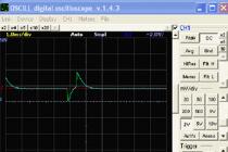
5) The inductance of the output choke is 4.9 μH, the current is 40A, respectively. We need it so that there are no huge current ripples at the output of our block, in the process of debugging I will show work with and without it on the oscilloscope, everything will become clear.
The calculation took 5 minutes, if someone has questions, then ask in the comments or PM - I'll tell you. In order not to look for the program itself, I suggest downloading it from the cloud using the link. And my deep gratitude to the Old Man for his work!
The next logical step is to calculate the output inductor for the half-bridge, which is exactly the one at 4.9 uH.
Calculation of winding parameters for the output choke
We received the input data in the previous paragraph when calculating the transformer, This:1) Inductance - 4.9 uH;
2) Rated current - 40A;
3) Amplitude in front of the throttle - 18V;
4) Voltage after the throttle - 15V.
We also use the program from the Old Man (all of them are in the link above) and get the following data:

Figure 3 - Calculated data for winding the output choke
Now let's run through the results:
1) According to the input data, there are 2 nuances: the frequency is chosen the same on which the converter operates, I think this is logical. The second point is related to the current density, I will immediately note - throttle should be hot! That's just how much we already determine, I chose a current density of 8A / mm 2 to get a temperature of 35 degrees, this can be seen in the output (marked in green). After all, as we remember, according to the requirements at the output, a “cold SMPS” is needed. I would also like to note for beginners a perhaps not entirely obvious point - the choke will heat up less if a large current flows through it, that is, at a rated load of 40A, the choke will have minimal heating. When the current is less than the rated current, then for a part of the energy it starts to work as an active load (resistor) and turns all excess energy into heat;
2) Maximum induction, this is a value that must not be exceeded, otherwise the magnetic field will saturate the core and everything will be very bad. This parameter depends on the material and its overall dimensions. For modern pulverized iron cores, the typical value is 0.5-0.55 T;
3) Winding data: 9 turns are wound with a scythe of 10 strands of wire with a diameter of 0.8 mm. The program even roughly indicates how many layers it will take. I will wind in 9 cores, because. then it will be convenient to divide a large braid into 3 “pigtails” of 3 cores and solder them on the board without any problems;
4) Actually, the ring itself on which I will wind it has dimensions - 40/24/14.5 mm, it is enough with a margin. Material No. 52, I think many have seen yellow-blue rings in ATX blocks, they are often used in group stabilization chokes (DGS).
Calculation of the standby power supply transformer
The functional diagram shows that I want to use the “classic” flyback on the TOP227 as a standby power supply, all PWM controllers, indications and cooling system fans will be powered from it. I realized that the fans will be powered from the duty room only after some time, so this moment is not displayed on the diagram, but nothing is real-time development))Let's adjust our input data a bit, what do we need:
1) Output windings for PWM: 15V 1A + 15V 1A;
2) Self-power output winding: 15V 0.1A;
3) Output winding for cooling: 15V 1A.
We get the need for a power supply with a total power - 2*15W + 1.5W + 15W = 46.5W. This is normal power for TOP227, I use it in small SMPS up to 75 W for all kinds of battery chargers, screwdrivers and other rubbish, for many years, which is strange, not one has yet burned out.
We go to another program of the Old Man and consider the transformer for the flyback:

Figure 4 - Calculated data for the standby power transformer
1) The choice of the core is justified simply - I have it in the amount of the box and it draws the same 75 W)) Data on the core. It is made of N87 material and has a gap of 0.2 mm on each half or 0.4 mm of the so-called full gap. This core is directly intended for chokes, and for flyback converters this inductance is just a choke, but I won’t get into the wilds yet. If there was no gap in the half-bridge transformer, then it is mandatory for the flyback converter, otherwise, like any inductor, it will simply go into saturation without a gap.
2) Data on the key 700V "drain-source" and 2.7 Ohm of channel resistance are taken from the datasheet on TOP227, this controller has a power switch built into the microcircuit itself.
3) I took the minimum input voltage a little with a margin - 160V, this is done so that if the power supply itself is turned off, the duty room and indication remain in operation, they will report an emergency low supply voltage.
4) Our primary winding consists of 45 turns of 0.335 mm wire into one core. The secondary power windings have 4 turns and 4 cores with a wire of 0.335 mm (diameter), the self-supply winding has the same parameters, so everything is the same, only 1 core, because the current is an order of magnitude lower.
Calculation of the power choke of the active power corrector
I think the most interesting part of this project is the power factor corrector, because. there is quite little information on them on the Internet, and there are even fewer working and described schemes.We choose a program for calculation - PFC_ring (PFC is in Basurmansk KKM), we use the following inputs:
1) Input supply voltage - 140 - 265V;
2) Rated power - 600 W;
3) Output voltage - 380V DC;
4) Operating frequency - 100 kHz, due to the choice of PWM controller.

Figure 5 - Calculation of the power choke of the active PFC
1) On the left, as usual, we enter the initial data, setting the minimum threshold to 140V, we get a unit that can operate at a mains voltage of 140V, so we get a “built-in voltage regulator”;
The circuitry of the power section and control is quite standard, if you suddenly have questions, then feel free to ask in the comments or in private messages. I will try my best to answer and explain.
Switching power supply circuit board design
So I got to the stage, which remains something sacred for many - the design / development / tracing of the printed circuit board. Why do I prefer the term "design"? It is closer to the essence of this operation, for me the “wiring” of the board is always a creative process, like an artist painting a picture, and it will be easier for people from other countries to understand what you are doing.The board design process itself does not contain any pitfalls, they are contained in the device for which it is intended. In fact, power electronics does not put forward some wild number of rules and requirements against the background of the same microwave analogue or high-speed digital data buses.
I will list the basic requirements and rules relating specifically to power circuitry, this will allow the implementation of 99% of amateur designs. I won’t talk about the nuances and “tricks” - everyone should fill their own bumps, gain experience and already operate with it. And so we went:
A little about the current density in printed conductors
Often people do not think about this parameter and I have seen where the power part is made with 0.6 mm conductors with 80% of the board area simply empty. Why do this is a mystery to me.
So what current density can be taken into account? For an ordinary wire, the standard figure is 10A / mm 2, this limitation is tied to the cooling of the wire. You can also pass a larger current, but before that, lower it into liquid nitrogen. Flat conductors, like on a printed circuit board, for example, have a large surface area, it is easier to cool them, which means that you can afford high current densities. For normal conditions with passive or air cooling, it is customary to take into account 35-50 A / mm 2, where 35 is for passive cooling, 50 is in the presence of artificial air circulation (my case). There is one more figure - 125 A/mm 2 , this is a really big figure, not all superconductors can afford it, but it is achievable only with immersion liquid cooling.
I encountered the latter while working with a company engaged in engineering communications and server design, it was the design of the motherboard that fell to my lot, namely the part with multi-phase power and switching. I was very surprised when I saw a current density of 125 A / mm 2, but they explained to me and showed this possibility at the stand - then I realized why entire racks with servers are immersed in huge pools of oil)))
In my piece of iron, everything is simpler, 50 A / mm 2 figure is quite adequate for itself, with a copper thickness of 35 microns, the polygons will provide the desired cross section without any problems. The rest was for the general development and understanding of the issue.
2) The length of the conductors - in this paragraph there is no need to equalize the lines with an accuracy of 0.1 mm, as is done, for example, when "wiring" the DDR3 data bus. Although it is still highly desirable to make the length of the signal lines approximately equal to the length. +-30% of the length will be enough, the main thing is not to make HIN 10 times longer than LIN. This is necessary so that the fronts of the signals do not shift relative to each other, because even at a frequency of only a hundred kilohertz, a difference of 5-10 times can cause a through current in the keys. This is especially true with a small value of "dead time", even at 3% for TL494 this is true;
3) The gap between the conductors - it is necessary to reduce leakage currents, especially for conductors where the RF signal (PWM) flows, because the field in the conductors is strong and the RF signal, due to the skin effect, tends to escape both to the surface of the conductor and beyond its limits. Usually a gap of 2-3 mm is sufficient;
4) Galvanic isolation gap - this is the gap between galvanically isolated sections of the board, usually the breakdown requirement is about 5 kV. To break through 1 mm of air, about 1-1.2 kV is needed, but with us a breakdown is possible not only through air, but also through textolite and a mask. In the factory, materials that undergo electrical testing are used and you can sleep peacefully. Therefore, the main problem is air and from the above conditions, we can conclude that about 5-6 mm of clearance will be enough. Basically, the division of polygons under the transformer, because. it is the main means of galvanic isolation.
Now let's go directly to the design of the board, I will not talk in this article in super detail, and in general it is not much to write a whole book of text of desire. If there is a large group of people who want it (I’ll do a survey at the end), then I’ll just shoot videos on the “wiring” of this device, it will be both faster and more informative.
Stages of creating a printed circuit board:
1) The first step is to determine the approximate dimensions of the device. If you have a ready-made case, then you should measure the footprint in it and start from it in the dimensions of the board. I plan to make a case made to order from aluminum or brass, so I will try to make the most compact device without losing quality and performance characteristics.

Figure 9 - We create a blank for the future board
Remember - the dimensions of the board must be a multiple of 1 mm! Or at least 0.5 mm, otherwise you will still remember my testament of Lenin, when you assemble everything in panels and make a blank for production, and the designers who will create the case according to your board will shower you with curses. Do not create a board with dimensions ala "208.625 mm" unless absolutely necessary!
P.S. thanks tov. Lunkov for the fact that he nevertheless conveyed this bright idea to me))
Here I did 4 operations:
A) I made the board itself with overall dimensions of 250x150 mm. While this is an approximate size, then I think it will shrink noticeably;
b) Rounded the corners, because in the process of delivery and assembly, sharp ones will be killed and wrinkled + the board looks nicer;
c) Placed mounting holes, not metallized, with a hole diameter of 3 mm for standard fasteners and racks;
d) Created a class "NPTH", in which I defined all non-plated holes and created a rule for it, creating a gap of 0.4 mm between all other components and components of the class. This is the technological requirement of "Rezonit" for the standard accuracy class (4th).

Figure 10 - Creating a rule for non-plated holes
2) The next step is to make the arrangement of the components, taking into account all the requirements, it should already be very close to the final version, because the larger part will now be determined by the final dimensions of the board and its form factor.

Figure 11 - Primary placement of components completed
I installed the main components, they will most likely not move, and therefore the overall dimensions of the board are finally determined - 220 x 150 mm. The free space on the board is left for a reason, control modules and other small SMD components will be placed there. To reduce the cost of the board and ease of installation, all components will be only on the top layer, respectively, and there is only one silk-screen printing layer.

Figure 13 - 3D view of the board after placing the components
3) Now, having determined the location and overall structure, we arrange the remaining components and “divide” the board. The design of the board can be done in two ways: manually and with the help of an autorouter, having previously described its actions with a couple of dozen rules. Both methods are good, but I will do this board with my hands, because. there are few components and there are no special requirements for line alignment and signal integrity here and should not be. This will definitely be faster, autorouting is good when there are a lot of components (from 500 onwards) and the main part of the circuit is digital. Although if someone is interested, I can show you how to "breed" the boards automatically in 2 minutes. True, before that it will be necessary to write the rules all day, heh.
After 3-4 hours of “witchcraft” (half the time I drew the missing models) with temperature and a cup of tea, I finally parted the board. I didn’t even think about saving space, many will say that the dimensions could be reduced by 20-30% and they will be right. I have a piece copy and wasting my time, which is clearly more expensive than 1 dm 2 for a two-layer board, was just a pity. By the way, about the price of the board - when ordering at Resonit, 1 dm 2 of a two-layer board of a standard class costs about 180-200 rubles, so you can’t save a lot here, unless of course you have a batch of 500+ pieces. Based on this, I can advise - do not pervert with a decrease in area, if class 4 and no requirements for dimensions. And here is the output:

Figure 14 - Board design for a switching power supply
In the future, I will design a case for this device and I need to know its full dimensions, as well as be able to “try on” it inside the case so that at the final stage it doesn’t turn out, for example, that the main board interferes with the connectors on the case or indication. To do this, I always try to draw all the components in a 3D form, the output is this result and a file in the .step format for my Autodesk Inventor:

Figure 15 - 3D view of the resulting device

Figure 16 - 3D view of the device (top view)
Now the documentation is ready. Now it is necessary to generate the necessary package of files for ordering components, I have all the settings already registered in Altium, so everything is unloaded with one button. We need Gerber files and an NC Drill file, the first one stores information about the layers, the second one stores the drilling coordinates. You can see the file for uploading documentation at the end of the article in the project, it all looks something like this:
Figure 17 - Forming a documentation package for ordering printed circuit boards
After the files are ready, you can order boards. I will not recommend specific manufacturers, for sure there are better and cheaper ones for prototypes. I order all boards of the standard class of 2,4,6 layers in Rezonit, in the same place 2 and 4-layer boards of the 5th class. Boards of class 5, where 6-24 layers are in China (for example, pcbway), but HDI and class 5 boards with 24 or more layers are only in Taiwan, all the same, the quality in China is still lame, and where the price tag is not lame already not so pleasant. It's all about prototypes!
Following my convictions, I go to Resonit, oh, how many nerves they frayed and blood they drank ... but lately they seem to have corrected themselves and began to work more adequately, albeit with kicks. I form orders through my personal account, enter data about the fee, upload files and send. I like their personal account, by the way, it immediately considers the price and by changing the parameters you can achieve a better price without losing quality.
For example, now I wanted a board on a 2 mm PCB with 35 µm copper, but it turned out that this option is 2.5 times more expensive than the option with 1.5 mm PCB and 35 µm - so I chose the latter. To increase the rigidity of the board, I added additional holes for the racks - the problem is solved, the price is optimized. By the way, if the board went into a series, then somewhere on 100 pieces this difference would disappear by 2.5 times and the prices would become equal, because then a non-standard sheet was bought for us and spent without residue.

Figure 18 - The final view of the calculation of the cost of boards
The final cost is determined: 3618 rubles. Of these, 2100 is preparation, it is paid only once per project, all subsequent repetitions of the order go without it and pay only for the area. In this case, 759 rubles for a board with an area of 3.3 dm 2, the larger the series, the lower the cost, although now it is 230 rubles / dm 2, which is quite acceptable. Of course, it was possible to make urgent production, but I order often, I work with one manager and the girl always tries to push the order faster if the production is not loaded - as a result, with the “small series” option, it takes 5-6 days, it’s enough just to communicate politely and don't be rude to people. And I have nowhere to hurry, so I decided to save about 40%, which is at least nice.
Epilogue
Well, I have come to the logical conclusion of the article - obtaining circuitry, board design and ordering boards in production. In total there will be 2 parts, the first is in front of you, and in the second I will tell you how I installed, assembled and debugged the device.As promised, I share the source code of the project and other products of activity:
1) Project source in Altium Designer 16 - ;
2) Files for ordering printed circuit boards - . Suddenly you want to repeat and order, for example, in China, this archive is more than enough;
3) Device diagram in pdf - . For those who don't want to waste time installing Altium on their phone or for familiarization (high quality);
4) Again, for those who do not want to install heavy software, but it is interesting to twist the piece of iron, I post a 3D model in pdf - . To view it, you must download the file, when you open it in the upper right corner, click "trust the document only once", then we poke in the center of the file and the white screen turns into a model.
I would also like to ask the opinion of readers ... Now the boards are ordered, the components are also - in fact there are 2 weeks, what should I write an article about? In addition to such "mutants" as this one, sometimes you want to make something miniature, but useful, I presented several options in the polls, or offer your own option, probably in a personal message, so as not to clutter up the comments.
Only registered users can participate in the survey. , Please.