The photodiode can operate in photodiode and galvanic modes.
V photodiode p-n mode the junction is shifted by a reverse voltage, the value of which depends on a particular photodiode from units to hundreds of volts, the greater the bias, the faster it will work, and more currents will flow through it.
The disadvantage of the photodiode mode is that with an increase in the reverse current, as a result of an increase in voltage or lighting, the noise level increases, and the level of the useful signal as a whole remains constant, it is believed that in this mode the diode has a shorter time constant.
Photodiode switching circuit.
The above circuit for connecting a photodiode is universal and suitable for testing and selection, in relation to the final circuit of its design.
By changing the position of the trimmer, in the above diagram, you can test and select the optimal mode of operation of the photodiode.
By changing the resistance of the resistor from minimum to maximum, you can choose best mode photodiode bias.
Turning the resistor to a minimum, closing the movable contact to ground, we transfer the circuit to photovoltaic mode.
You can try the operation of the photodiode in forward bias (it will still react to light), for this you need to change switching circuit by flipping the diode.
A resistance of 50 ohms should not damage the photodiode, but in terms of the variable component, it turns out to be connected in parallel with the load (less than 5 kΩ), and the useful signal practically does not weaken. The capacitor relieves us of the constant component. If we receive a pulsed signal, then it is better to get rid of the constant component, which changes depending on the background illumination, immediately, there is no point in amplifying it.
 Another standard photodiode switching circuit is shown in the figure.
In this installation, to reduce the influence of noise and interference, buffer capacitors in the power circuit, a storage capacitor C3 and an integrating circuit R2C4 at the output are added to the circuit.
C1- electrolytic capacitor large capacity C = 100 μF, C2 - fast ceramic 0.1 μF, C3, C4 - ceramic 100 pF each, R1 - 8 kΩ, R2 - 5.6 kΩ.
To achieve maximum speed, the load must be either a cascade with a common base or a high-speed opamp connected according to the current-voltage converter circuit. These amplifiers have a minimum input impedance.
Practical circuitry for switching on a biased photodiode.

Practical circuitry for switching on a biased photodiode.
The R value of the filter is selected depending on the exposure of the photodiode in the working version with installed optics, the azimuth direction (south, west, etc.) in different directions, different illumination from the sun, is taken into account.
Capacitance Cf = 0.1mkF also closes the photodiode circuit at high frequency to ground.
Instead of Rn, you can put a choke or a transformer, you need to look to see if there will be distortions or puffs of pulses or other pitfalls.
The inclusion of a photodiode in a cascade with a common base.

Scheme for connecting the PD 263 photodiode to a cascade with a common base.
In a circuit with OB - the base separates the input and output circuits, and practically eliminates the effect of the output voltage on the input of the circuit (like the screen grid in a pentode), therefore, it is possible to increase the load resistance and obtain a larger voltage swing at the output of the circuit without sacrificing speed.
Principle of operation
Figure 2 shows a diagram showing the principle of operation of detectors with a reverse biased photodiode. The magnitude of the generated photocurrent depends on the luminous flux and the radiation wavelength. When connecting a load resistor, this value can be observed with an oscilloscope. The function of the RC filter is to suppress high frequency noise from the power supply.

Fig. 3 Amplified detector circuit
When using a photodetector circuit with an amplifier, the user can select the operating mode of the photodiode (photovoltaic or photodiode). Each mode has its own advantages:
Photovoltaic mode: In photovoltaic mode, no voltage is applied to the diode and the potential at input A of the op-amp is equal to the potential at point B. In this mode, the dark current is negligible.
Photodiode mode: In the photodiode mode, a reverse bias voltage is applied to the pn junction, which reduces the junction capacitance and increases the bandwidth. The gain depends on the resistor feedback(R f). The bandwidth of the detector is determined by the formula:

Where GBP is the product of the gain by the bandwidth of the op amp, C D is the sum of the junction capacitance and the amplifier.
Modulation frequency
The noise spectral density of most detectors, including PbS, PbSe, HgCdTe (MCT) and InAsSb, has a 1 / f dependence (noise decreases with increasing frequency), which has a significant effect on the time constant at low frequencies.
Thus, the modulation frequency (rate of change in intensity) of radiation affects the sensitivity of the device. The optimal values of the characteristics of the photodetector are achieved at the frequency:
Battery life
When using a battery-operated photo detector, it is important to understand what the battery life is and how it affects the performance of the detector. The detector output current is directly proportional to the incident radiation flux. Most users convert this current to voltage using a matched load. The resistance value is approximately equal to the gain of the circuit. For high speed detectors such as, a 50 ohm load must be used to match the impedance of standard coaxial cables. This will reduce back reflections and improve the quality of the output signal.
The battery life is directly related to the current in the detector. Most battery manufacturers express battery life in mAh (milliampere-hour). For example, if the battery is rated at 190 mAh, it will operate for 190 hours at a current consumption of 1.0 mA.
Let the source, the radiation of which falls on the detector, operate at a wavelength of 780 nm with an average power of 1 mW. The sensitivity of the detector at a given wavelength is 0.5 A / W. The photocurrent can be calculated using the formula:
![]()
Thus, the battery life is:

or 16 days of continuous work. With a decrease in the average power of the incident radiation to 10 μW, the service life of the same battery will increase to 4 years of continuous operation. Using the recommended matched load of 50 ohms, the photocurrent (0.5 mA) is converted to voltage: If the incident power is reduced to 40 µW, the output voltage becomes 1 mW. For some measuring devices, this value may be too small, so a compromise must be found between battery life and measurement accuracy.

When using battery-powered detectors, low-intensity radiation should be used, taking into account the minimum required voltage level. It is also important to remember that the battery will not stop producing current immediately as it approaches the end of its life. First, the battery voltage will drop and the electrical potential applied to the photodiode will decrease. This, in turn, will lead to an increase in detector response time and a decrease in bandwidth.
Therefore, it is important to ensure that the battery provides sufficient voltage for optimal detector performance.
For applications in which detectors are continuously exposed to a source of sufficiently high power, or constant battery replacement is unacceptable, the company Thorlabs offers adapter and power supply. The disadvantage of this option is noise, which will add to the output signal and can increase the measurement error.
Lead sulfide (PbS) and lead selenide (PbSe) detectors are widely used for detecting radiation in the range from 1000 to 4800 nm. Whereas a photodiode generates a current when exposed to light, a photoresistor changes its resistance under irradiation. Although PbS and PbSe detectors can be used at room temperature, temperature fluctuations will affect the dark resistance, sensitivity and performance of the instrument.
Principle of operation
When light is absorbed in a photoconductive material, excess charge carriers arise, leading to an increase in conductivity and a decrease in resistance. A change in resistance will change the magnitude of the measured voltage. In fig. a diagram showing the principle of operation of detectors based on photoconductive materials is presented. It should be noted that the presented circuit is not recommended for practical use due to the presence of low-frequency noise.
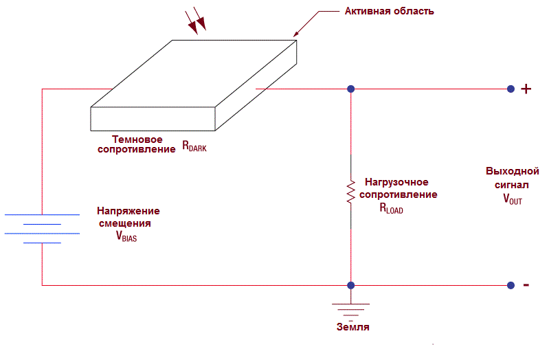
The detection mechanism is based on the conductivity of a thin film of the photosensitive element. The signal at the detector output in the absence of incident radiation is determined by the equation:
The voltage change at the output ΔV OUT occurs due to the change in resistance ΔR Dark when light hits the active area of the sensor:
Frequency response
For detectors, the dependence of the sensitivity on the modulation frequency of light has the form:
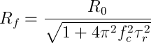
Where f c is the modulation frequency, R 0 is the sensitivity at a frequency of 0 Hz, τ r is the rise time.
Exposure to temperature
The light-sensitive element of PbS and PbSe detectors is a thin film on a glass substrate. The shape and active area of the photoconductive element change depending on the operating conditions, thus changing other characteristics as well. In particular, the sensitivity of the detector will vary with the operating temperature.
Cooling the detector will shift the spectral sensitivity range to longer wavelengths. For optimum results, it is recommended to use the presented detectors in a controlled environment.
Circuit of a detector based on a photoconductive material with an amplifier
Due to the noise characteristics, it is preferable to include the photoresistor in the AC circuit. When the photoresistor is connected to the DC link, the noise due to the applied voltage will increase with increasing voltage, thus limiting the sensitivity of the detector. A preamplifier should be used to maintain stability and obtain high signal gain values.

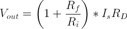
According to the diagram (Fig. Above), the operational amplifier (op-amp) seeks to equalize the potentials at points A and B using a feedback loop. The voltage difference at the input of the op-amp is amplified and transmitted to the output. It should be noted that the high-pass filter at the amplifier input does not pass the DC signal. In addition, the load resistance must be equal to the dark resistance of the detector in order to obtain the maximum signal. The value of the voltage of the power supply (+ V) should be such that the value of the signal-to-noise ratio is optimal and approaches unity. Some tasks require more high level voltage, which will increase the noise level. The output voltage is determined by the formula:
Signal to noise ratio
Since the noise level of the detector is inversely proportional to the modulation frequency of the signal, the noise will increase at low frequencies. The signal at the detector output increases linearly with increasing bias voltage, but the noise performance is not very dependent on the bias voltage at its low level. Upon reaching a certain level bias voltage, the detector noise will begin to increase linearly with increasing voltage. At high voltages, the noise will start to grow exponentially, decreasing the signal-to-noise ratio. To ensure the optimal signal-to-noise level, it is necessary to adjust the signal modulation frequency and offset voltage.
Dark Resistance
Dark resistance is the resistance of the detector when there is no illumination. It should be noted that the dark resistance will increase or decrease as the temperature changes. Cooling the detector will lower the dark resistance value.
Detective ability (D) and specific detectivity (D *)
Detectability (D) is another quantity used to assess the efficiency of a photodetector. Detectability characterizes sensitivity and is inversely proportional to noise equivalent power (NEP):
![]()
The higher the detectability value, the higher the sensitivity, that is, the detector is able to register weak signals. Detectability depends on the wavelength of the incident photons.
The NEP of a detector, and hence its detectivity, is dependent on the active region, so comparing the properties of the two detectors is not an easy task. To get rid of this dependence, the specific detectivity (D *) is used, which does not depend on the detector area and is used to assess the efficiency of the photodetector. In the equation below, A is the area of the photosensitive area.

2D Position Sensing Sensors
Overview
Two-dimensional position-sensitive sensors measure the position, travel distance or incidence angles of the beam, and they can also be used as feedback in alignment systems, for example, to control the position of mirrors, focusing a microscope, etc. The detector determines the position of the light spot based on the proportional distribution of the photocurrent generated at the point of incidence of the light beam. There are two types of 2D position-sensitive sensors: two-sided electrodes and four-sided electrodes.
Sensors with double-sided electrodes have resistive layers deposited on both sides of the substrate. The sensor has four leads. The photocurrent is divided into two input and two output components. The distribution of the output currents determines the position of the Y coordinate, and the distribution of the input currents determines the X coordinate of the beam position.

Sensors with a four-sided arrangement of electrodes have one sensitive resistive layer located on one side of the substrate. Such sensors are much cheaper than sensors with a double-sided arrangement of electrodes. However, the linearity of the response of these sensors decreases as the beam moves away from the center. This is due to the location of the anodes along the perimeter of the sensor, especially the nonlinearity is noticeable in the corners of the sensor, where the anodes approach each other. Company Thorlabs uses one of the variants of sensors with a four-sided arrangement of electrodes - a sensor in the form of a "pad". The model of such a sensor is shown in the figure above. The anodes are moved to the corners of the sensor, the figured shape of the electrodes compensates for signal distortions near the perimeter. This model has linearity at the level of sensors with double-sided electrodes, but at a much lower cost.
The principle of calculating the position of the beam
PDP90A detector from the company Thorlabs equipped with a circuit for calculating Δx, Δy and the sum of signals according to the formulas:

According to these formulas, the distance in length units can be calculated using the equations:

where x and y are the distance from the center to the edge of the sensor, Lx and Ly are the characteristic dimensions of the resistive layer. For PDP90A detector Lx = Ly = 10 mm. It should be noted that the dimensions of the resistive layer do not correspond to the dimensions of the active region of the sensor. The active area is indicated in the figure in gray.
Positioning error
Unlike quadrant sensors, where overlap of all four active regions is required, the presented sensors provide information on the location of the beam at any point of the detector, regardless of the shape, size, and power distribution in the beam. The sensor detects the position of the center of the spot of light as long as the spot is on the light-sensitive area. If part of the light spot leaves the light-sensitive surface, it will shift the center and measurements will become unreliable.
Errors in beam position measurements can also be caused by ambient light levels. To reduce errors, measurements are best performed in the dark. Using focusing optics and apertures will also reduce ambient light errors.
Permission
The resolution of the position-sensitive detector is the minimum detectable displacement of the light spot on the surface of the sensor sensor. Resolution (ΔR) depends on both the size of the resistive layer (L x or L y) and the signal-to-noise ratio (S / N). The signal-to-noise ratio of this system can be defined as the ratio of the sum of the output signals (Vo) to the noise voltage (e n). The noise at the output of the PDP90A detector is<2 мВ (двойная амплитуда сигнала) или 300 мкВ (среднеквадратичное значение).
Where
ΔR - resolution,
Lx is the characteristic size of the resistive layer,
e n - noise voltage at the detector output,
Vo is the sum of the output voltages.
For PDP90A detector:

For optimal results, the V o value must be increased to 4 V, which will provide a detector resolution of 0.750 µm. To do this, it is necessary to monitor the total output signal (SUM) of the sensor and at the same time adjust the intensity of the incident radiation until the voltage at the output is equal to 4 V. A voltage greater than 4 V will lead to system saturation and, therefore, to measurement errors. The supplied software makes it easy to monitor the voltage level. If the total voltage is higher than the saturation level, the slider displaying the total voltage level will turn red. In this case, it is necessary to reduce the radiation intensity to a level at which the color of the slider turns green. This value will correspond to 4 V output voltage.
Position-sensitive detector based on quadrant photodiodes
The sensor of such a detector consists of four identical quadrant photodiodes, which are separated by a gap of ~ 0.1 mm and together form a circular detection zone for determining the position of the incident beam (in 2D format). When light hits the sensor, a photocurrent is generated in each area (in Fig. Q1, Q2, Q3 and Q4). On the basis of these signals, the differential signals are calculated using the ADC. The sum of all four signals for normalization is also calculated. The normalized coordinates (X, Y) of the beam position are determined using the equations:

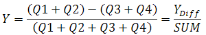

If a symmetric beam falls into the center of the sensor, then the system at the output will register 4 identical photocurrents, i.e. the difference signals will be equal to 0, and the normalized coordinates (X, Y) = (0, 0). The photocurrents will change if the beam is shifted relative to the center. In this case, the differential currents will not wound 0.
Quadrant photodiode detectors are very accurate and perfect for auto-alignment systems. However, it is necessary to monitor the shape and distribution of the intensity in the beam, since this type of detector is sensitive to these parameters. For beams where the power distribution is not Gaussian, the center will be determined based on the power distribution (not the geometric center of the beam). For such beams, it is preferable to use the detectors described in the previous paragraph.
Avalanche photodiodes in Geiger mode have the ability to detect single photons. Sensitivity at the level of single photons can be achieved by increasing the bias voltage above the breakdown voltage (point A in Fig. 4). The avalanche photodiode will remain in a metastable state until a photon is absorbed, which will generate an avalanche (point B). This avalanche is quenched by an active photodiode quenching circuit (point C) that lowers the bias voltage to values below the breakdown voltage (V BR).

Fig. 4: Current-voltage characteristic of an avalanche photodiode in Geiger mode
The high offset voltage can then be restored. During this process, which is known as diode dead time, the avalanche photodiode is insensitive to any incident photons. When a diode is in a metastable state, avalanches can form spontaneously. If the spontaneous formation of avalanches occurs chaotically, then the recorded signal is called a dark count. If the spontaneous formation of avalanches in time correlates with pulses from incident photons, then such a signal is called a post-pulse. To avoid registration of afterpulses during measurements, you can enter additional dead time by software (using software), which will cause the counter to ignore all pulses that have occurred during this time.
Basic characteristics and concepts
Geiger mode
In this mode, the diode operates at a bias voltage higher than the breakdown voltage. Consequently, one electron-hole pair (generated as a result of photon absorption or thermal fluctuations) can cause an avalanche process.
Dark count rate
This is the average of the recorded counts in the absence of incident radiation, which determines the minimum count rate at which the recorded signal is mainly caused by real photons. The registration of false photons is mainly related to thermal fluctuations and thus can be avoided by using cooled detectors.
Active damping occurs when the discriminator detects the occurrence of an avalanche current and sharply decreases the bias voltage to values below the breakdown voltage. In preparation for recording the next photon, the bias voltage increases again to values above the breakdown voltage.
Dead time- this is the time interval that the detector needs to restore the state at which it can register events without distortion. During this time, he does not see the incident photons. The part of the dead time associated with the active quenching circuit can be defined as the ratio of transmitted photons to incident photons.
Afterpulses
During the avalanche process, some charges can be captured by traps. When released, these charges can lead to the formation of an avalanche. Such "false events" are called afterpulses. The lifetime of such trapped charges is on the order of several tenths of a microsecond. Consequently, the occurrence of afterpulses is more likely immediately after a pulse from a real photon.
Basic models of photo detectors from Thorlabs
The table shows the models of photodetectors from the company Thorlabs. Models located in the same row are equipped with the same photosensitive elements.
|
Operating wavelength range |
Material | |||||
|
a Calibrated photodiode b TO-46 package Principle of operation Since the appearance of the first commercial PMTs in 1940, this type of detector has remained one of the most popular in experiments that require fast response times and high sensitivity. Today PMTs are indispensable for research in analytical chemistry, elementary particle physics, astronomy, atomic and molecular physics, as well as in medicine and control of production processes. Photomultiplier tubes (PMTs) are sensitive, high gain detectors whose output current is proportional to the incident radiation. The PMT consists of a glass vacuum tube in which a photocathode (photoemission material), 8-14 dynodes (secondary emission) and an anode (collector of secondary electrons) are located. If a photon with a sufficiently high energy (i.e., with an energy greater than the binding energy of the electrons of the photocathode material) falls on the photocathode, then it is absorbed and an electron is emitted (photoelectric effect). Since the potential on the first dynode is higher than the potential on the cathode (a potential difference is created between these elements), the released electron is accelerated in the electric field and directed to the dynode system, where, due to the secondary (shock) electron emission, an electron avalanche is formed. entering the anode. As a rule, each dynode has a potential that is 100 - 200 V higher than the potential of the previous dynode. The anode current is converted into voltage, for this a low-resistance load is connected to the circuit between the anode and ground. PMT and from the company Thorlabs use a transimpedance amplifier (TIA) to convert anode current (nA or μA) to voltage (mV or V). Modules, and do not contain a transimpedance amplifier. For example, if the PMT consists of 8 dynodes, as shown in Fig. below and each electron leads to the appearance of 4 secondary electrons, then the current amplification after the dynode system will be 4 8 ≈ 66,000. In the given example, each photoelectron leads to the appearance of an avalanche with a charge Q = 4 8 e, which comes to the anode. The voltage pulse in this case is equal to V = Q / C = 4 8 e / C, where C is the capacitance of the anode. If the capacitance is 5 pF, then the output pulse voltage will be 2.1 mV.
Spectral sensitivity When choosing a photomultiplier, it is necessary to pay attention to the material of the photocathode, since it defines the long-wavelength limit of spectral sensitivity. The shortwave boundary is determined by the material of the window. Today, various types of photomultipliers are manufactured to operate in the UV to IR range, while using different materials for the photocathode, each of which is designed to operate in a specific spectral range. Quantum efficiency (QE) is a percentage value that characterizes the ability of a PMT to convert incident photons into electrons. For example, QE is 20%. This means that one of the 5 photons incident on the photocathode will result in the appearance of photoelectrons. For photon counting problems, it is desirable to have a PMT with a high quantum efficiency. Since QE depends on the wavelength, it is necessary to select a PMT with the maximum quantum efficiency in the spectral range of interest. It should be noted that photocathodes for the visible region of the spectrum, as a rule, have QE<30%. The quantum efficiency of the PMT can be calculated using the formula:
where S is the integral sensitivity [A / W], λ is the wavelength [nm]. PMT configuration There are two main photomultiplier configurations available: the entrance window is located at the end or on the side wall of the vacuum flask. In the case when the entrance window is located at the end, the PMT is equipped with semitransparent photocathodes and is characterized by a large active region area, spatial homogeneity, and higher performance in the blue and green regions of the spectrum. This configuration is preferred for applications requiring wide spectral sensitivity such as spectroscopy. The photomultiplier with a side window uses opaque photocathodes, this configuration is most often used when working in the UV and IR ranges. The side window configuration is less expensive than the end window configuration and is often used for applications requiring high quantum efficiency such as scintillation measurements. 8-14 dynodes are arranged linearly or in a circle. With a linear arrangement (as shown in the figure), the PMT has a short response time, high resolution and linearity. Dynodes are arranged in a circle in a photomultiplier with a side window and in some photomultipliers with an end window, while the system has a compact size and a short response time. Gain PMTs are unique in that they are able to amplify very weak signals from the photocathode to a detectable level above the readout noise without introducing significant interference. Dynodes are responsible for amplifying the signal in the PMT, and the gain depends on the applied voltage. PMT can operate at voltages exceeding the values recommended by the manufacturer, while providing a gain 10-100 times higher than specified in the specification. When operating in this mode, the PMT is not negatively affected if the anode current is below the maximum permissible values. Dark current In the case of an ideal PMT, all signals produced by the photocathode are due to light entering the tube. However, real PMTs generate current even in the absence of incident radiation. The signal generated by the PMT in the absence of light is called dark current. This signal greatly reduces the signal-to-noise ratio of the PMT. The dark current is mainly due to the thermionic emission of electrons from the photocathode and the first few dynodes, and to a lesser extent by cosmic rays and radiation. PMTs designed for applications in the red region of the spectrum have higher dark currents than other PMTs due to the low electron binding energies in photocathodes that are sensitive in the red region of the spectrum. Thermionic emission depends on the temperature of the photocathode and the work function, which means that cooling the PMT can significantly reduce the dark current. When using a photomultiplier with thermoelectric cooling, condensation on the entrance window should be avoided, as moisture will reduce the amount of light falling on the photocathode. In addition, excessive cooling must be avoided, as this can lead to negative consequences: a decrease in the signal level or voltage at the cathode, because the resistance of the cathode film is inversely proportional to the temperature. Rise Time For experiments requiring high temporal resolution, the rise time should be short. The rise time of the anode current pulse is most often used as a characteristic of the speed of the PMT. Ultimately, the rise time of a pulse is determined by the propagation time of different electrons. It differs for several reasons. First, the initial velocities of the secondary electrons are different. since they are knocked out of the places of the material of the dynodes of different depths. Some electrons escaping have a nonzero initial energy, so they will reach the next dynode in a shorter time. The time of flight for electrons will also depend on the path length. As a result of all these effects, the rise time of the anode current pulse will decrease with increasing voltage as V -1/2. Other factors When working with PMTs, the electronics to be used should be carefully selected. Even small fluctuations in the high voltage applied between the cathode and anode can greatly affect the output signal. In addition, environmental conditions can also affect the operation of the PMT. Changes in temperature and humidity, as well as vibration, negatively affect the performance of the PMT. The PMT housing is also of great importance, it not only protects the tube from extraneous light, but also reduces the influence of external magnetic fields. A field with a magnetic induction of a few gauss can reduce the gain. This can be avoided by using a magnetic shield made of a material with high magnetic permeability. | ||||||

The main characteristics of a photodiode are: I - V characteristic, light and spectral.
Volt-ampere characteristics... In the general case (for any polarity U), the photodiode current is described by expression (1). This expression is the dependence of the photodiode current I f on the voltage on the photodiode U at different values of the radiation flux F, i.e. is the equation of the family of current-voltage characteristics of the photodiode. The graphs of the current-voltage characteristics are shown in Fig. 1.7 .
Rice. 1.7 I - V characteristic of the photodiode.
The family of current-voltage characteristics of the photodiode is located in quadrants I, III and IV. Quadrant I is a non-working area for a photodiode: in this quadrant, a forward voltage is applied to the p-n junction and the diffusion component of the current completely suppresses the photocurrent (I p - n >> I ph). Photocontrol via a diode becomes impossible.
Quadrant III is the photodiode region of the photodiode operation. A reverse voltage is applied to the p-n junction. It should be emphasized that in the operating range of reverse voltages, the photocurrent is practically independent of the reverse voltage and load resistance. The current-voltage characteristic of the load resistor R is a straight line, the equation of which is:
E arr - I f · R = U,
where U arr is the voltage of the reverse voltage source; U is the reverse voltage across the photodiode; I f - photocurrent (load current).
The photodiode and the load photoresistor are connected in series, i. E. the same current I ph flows through them. This current I f can be determined by the point of intersection of the current-voltage characteristics of the photodiode and the load resistor (Fig. 1.7 quadrant III) Thus, in the photodiode mode at a given radiation flux, the photodiode is a source of current I f with respect to the external circuit. The value of the current I f on the parameters of the external circuit (U arr, R) practically does not depend (Fig. 1.7.).
Quadrant IV of the family of current-voltage characteristics of the photodiode corresponds to the photovoltaic mode of operation of the photodiode. The points of intersection of the current-voltage characteristics with the voltage axis correspond to the values of the photo-EMF E ph or the open-circuit voltages U xx (R n = ∞) at different fluxes F. For silicon photodiodes, the photo-EMF is 0.5-0.55 V. current-voltage characteristics with the axis of currents correspond to the values of short-circuit currents I kz (R n = 0). Intermediate values of load resistance are determined by load lines, which for different values of R n come out of the origin at different angles. At a given current value, according to the current-voltage characteristics of the photodiode, you can select the optimal mode of operation of the photodiode in the photovoltaic mode (Fig. 1.8). In this case, the optimal mode is understood as the choice of such a load resistance, at which the greatest electrical power will be transmitted to R n.

Figure 1.8. I - V characteristic of a photodiode in the photovoltaic mode.
The load line R 1 corresponds to the optimal mode for the flow F1 (the area of the shaded rectangle with apex at point A, where the lines F1 and R 1 intersect, will be the largest - Fig. 1.8). For silicon photodiodes at optimal load, the voltage across the photodiode is U = 0.35-0.4 V.
Light (energy) characteristics of the photodiode Is the dependence of the current on the luminous flux I = f (F):

Rice. 1.9. Light characteristic of PD.
In the photodiode mode, the energy characteristic in the operating range of radiation fluxes is linear.
This suggests that almost all photocarriers reach the p-n junction and take part in the formation of a photocurrent, the loss of minority carriers for recombination does not depend on the radiation flux.
In the photovoltaic mode, the energy characteristics are represented by the dependences of either the short-circuit current I cc, or the photo-EMF E f on the radiation flux F. At high fluxes F, the law of variation of these dependences significantly deviates from linear (Fig. 1.10).
|
Figure 1.10 Light characteristics of PD
For the function Ic = f (Ф), the appearance of nonlinearity is associated with an increase in the voltage drop across the bulk resistance of the semiconductor base. The decrease in the photo-emf is explained by a decrease in the height of the potential barrier with the accumulation of excess charge of electrons in the n-region and holes in the p-region.
The diode mode has the following advantages in comparison with the generator mode:
· The output current in the photodiode mode does not depend on the load resistance; in the generator mode, the maximum input current can be obtained only with a short circuit in the load.
Photodiode mode is characterized by high sensitivity, big dynamic range conversion of optical radiation, high speed (barrier capacity p-n transition decreases).
The disadvantage of the photodiode operating mode is the dependence of the dark current (reverse current p-n transition) from temperature.
The main parameters are:
Dark current I t.
· Operating voltage U slave - the voltage applied to the diode in the photoconversion mode.
· Integral sensitivity K f.
A photodiode is a light-sensitive diode that uses light energy to create voltage. Widely used in household and industrial automatic systems control, where the switch is the amount of incoming light. For example, control of the degree of opening of blinds in a smart home system, based on the level of illumination
When light hits the photodiode, the energy of the light hitting the light-sensitive material creates a voltage that causes electrons to move through the P-N junction. There are two types of photodiodes: photovoltaic and photoconductive.
Photoconductive diodes
Such diodes are used to control electrical circuits to which the potential is supplied from the outside, that is, from an external source.
For example, they can regulate the switching on and off of street lights or open and close automatic doors.
In a typical circuit in which a photodiode is installed, the potential applied to the diode is reverse biased and slightly below the diode breakdown voltage. No current flows through such a circuit. When light hits the diode, the additional voltage that begins to move through the P-N junction causes the depletion region to narrow and allows current to flow through the diode. The amount of current passing is determined by the intensity of the light flux entering the photodiode.
Photovoltaic diodes
Photovoltaic diodes are the only voltage source for the circuit in which they are installed.
One example of such a photoelectric diode is a photoexposure meter used in photography to determine illumination. When light hits the light-sensitive diode in the exposure meter, the resulting voltage triggers measuring device... The higher the illumination, the more voltage is applied to the diode.
A special place in electrical engineering is occupied by photodiodes, which are used in different devices and devices. A photodiode is a semiconductor element similar in properties to a simple diode. Its reverse current directly depends on the intensity of the light flux incident on it. Most often, semiconductor elements with a pn junction are used as a photodiode.
Device and principle of operation
A photodiode is included in many electronic devices. Therefore, he gained wide popularity. An ordinary LED is a pn junction diode, the conductivity of which depends on the light incident on it. In the dark, the photodiode has the characteristics of a conventional diode.
1
- semiconductor junction.
2
- positive pole.
3
- photosensitive layer.
4
- negative pole.
When the light flux acts on the transition plane, photons are absorbed with an energy exceeding the limiting value, therefore, pairs of charge carriers - photocarriers are formed in the n-region.
When the photocarriers are mixed in the depth of the region "n", the main part of the carriers does not have time to recombine and passes to border p-n... At the transition, photocarriers are divided by an electric field. In this case, the holes go to the "p" region, and the electrons are not able to go through the transition, therefore they accumulate near the boundary of the pn transition, as well as the "n" region.
The reverse current of the diode is increased when exposed to light. The amount by which the reverse current rises is called photocurrent.
Photocarriers in the form of holes carry out a positive charge of the "p" region in relation to the "n" region. In turn, the electrons produce a negative charge in the "n" region relative to the "p" region. The resulting potential difference is called the photoelectromotive force, and is designated "E f". The electric current generated in the photodiode is reversed and is directed from the cathode to the anode. Moreover, its value depends on the amount of illumination.
Modes of operation
Photodiodes are capable of functioning in the following modes:
- Photogenerator mode. Without connecting a source of electricity.
- Photoconverter mode. With connection external source nutrition.
In work photogenerator Photodiodes are used in place of a power supply that converts sunlight into electrical energy. Such photogenerators are called solar cells. They are the main parts solar panels used in various devices, including spacecraft.
The efficiency of silicon-based solar cells is 20%; this parameter is much higher for film cells. An important property of solar cells is the dependence of the output power on the weight and area of the sensitive layer. These properties reach values of 200 W / kg and 1 kW / m 2.
When the photodiode functions as photoconverter , the voltage source is connected to the circuit with reverse polarity. In this case, reverse graphs of the current-voltage characteristics are used at different illumination levels.

The voltage and current at the load R n are determined on the graph by the intersections of the characteristics of the photodiode and the load line, which corresponds to the resistor R n. In the dark, the photodiode is equivalent to an ordinary diode in its action. The current in the dark mode for silicon diodes ranges from 1 to 3 microamperes, for germanium diodes from 10 to 30 microamperes.
Types of photodiodes
There are several different types of photodiodes that have their own advantages.
p – i – nphotodiode
V area p-n this diode has a section with high resistance and intrinsic conductivity. When exposed to light, pairs of holes and electrons are generated. The electric field in this zone has a constant value, there is no space charge.
This auxiliary layer significantly reduces the capacitance of the barrier layer and is not voltage dependent. This expands the operating frequency band of the diodes. As a result, the speed rises sharply, and the frequency reaches 10 10 hertz. The increased resistance of this layer significantly reduces the operating current in the absence of lighting. For the luminous flux to be able to penetrate the p-layer, it should not be thick.

Avalanche photodiodes
This type of diode is a high sensitivity semiconductor that converts lighting into an electric current signal using a photoelectric effect. In other words, these are photodetectors that amplify the signal due to the effect of avalanche multiplication.

1 - ohmic contacts 2 - antireflection coating
Avalanche photodiodes are more sensitive than other photodetectors. This makes it possible to use them for low light powers.
Superlattices are used in the design of avalanche photodiodes. Their essence lies in the fact that significant differences in the impact ionization of carriers lead to a drop in noise.
Another advantage of using similar structures is the localization of avalanche reproduction. It also reduces interference. In a superlattice, the thickness of the layers ranges from 100 to 500 angstroms.
Operating principle
At a reverse voltage close to the value of the avalanche breakdown, the photocurrent is sharply increased due to impact ionization of charge carriers. The action consists in the fact that the energy of the electron increases from the external field and can exceed the ionization limit of the substance, as a result of which the meeting of this electron with an electron from the valence band will lead to the appearance of a new pair of an electron and a hole. The charge carriers of this pair will be accelerated by the field and can facilitate the formation of new charge carriers.
Specifications
The properties of such light diodes can be described by some dependencies.
Volt-ampere
This characteristic is the dependence of the current strength at a constant flux of light on the voltage.

I- current M- multiplication factor U- voltage
Luminous
This property is the dependence of the diode current on lighting. As the light flux increases, the photocurrent increases.
Spectral
This property is the dependence of the diode current on the light wavelength, and is the width of the boundary zone.
Time constant
This is the time during which the photocurrent of the diode changes after the supply of light in comparison with the steady-state value.
Dark Resistance
This is the resistance value of the diode in the dark.
Inertia
Factors affecting this characteristic:
- Diffusion time of nonequilibrium charge carriers.
- Time of passage along the pn junction.
- Recharge period of the pn junction barrier capacity.
Scope of application
Photodiodes are the basic building blocks of many optoelectronic devices.
Integrated microcircuits (optoelectronic)
The photodiode can have a significant operating speed, but the current amplification factor is not more than unity. Due to the optical connection, microcircuits have significant advantages: perfect galvanic isolation of control circuits from powerful power circuits. At the same time, a functional connection is maintained between them.
Photo detectors with multiple elements
These devices in the form of a photodiode array, a scanistor, are new progressive electronic devices. Their optoelectronic eye with a photodiode can create a reaction to the spatial and brightness properties of objects. In other words, he can see his full visual image.
The number of light-sensitive cells is very large. Therefore, in addition to issues of speed and sensitivity, it is necessary to read information. All photodetectors with multiple photocells are scanning systems, that is, devices that allow you to analyze the space under investigation by sequential element-by-element viewing.
Photodiodes are also widely used in fiber optic lines, laser rangefinders. Recently, such light diodes have been used in positron emission tomography.
Currently, there are samples of photosensitive arrays consisting of avalanche photodiodes. Their effectiveness and scope depends on some factors.
The following factors turned out to be the most influencing:
- The total leakage current generated by adding noise and current in the absence of light.
- Quantum efficiency, which determines the fraction of incident quanta that lead to the emergence of current and charge carriers.